

The AI datacenter, Nvidia's integrated AI factory vs Broadcom's open fabric
The AI datacenter, Nvidia's integrated AI factory vs Broadcom's open fabric
Outlook post Nvidia's and Broadcom's AI events

Both Nvidia and Broadcom held their respective AI events last week, presenting two opposing viewpoints for the future of the AI datacenter. The former’s strategy is really to have customers run all their AI workloads on Nvidia’s vertically integrated solution, from the company’s GPUs and now also CPUs, to Nvidia’s server racks and networking, all powered by Nvidia software and libraries. The company has been building up an impressive software ecosystem over the years. Most famous is its CUDA GPU computing platform, allowing for the hyperfast general purpose programming languages C and C++ to execute on any of Nvidia’s GPUs, avoiding the need for cumbersome graphic programming techniques. Additionally, AI engineers get access to a wide variety of libraries to deploy and scale workloads on Nvidia GPUs. For example, data processing with Python pandas can now be accelerated on the company’s GPUs and Nvidia also offers inferencing libraries such as TensorRT-LLM and Triton Server to deploy trained AI models on Nvidia GPUs. These AI models can be developed with popular frameworks such as Pytorch and Tensorflow.
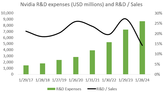
A lot of financial analysts have the impression that AI coding is happening in CUDA, which would give Nvidia a strong moat on the software side, but this is unfortunately not the case. Practically all AI code is written in Pytorch, which can run on top of CUDA, CPUs, and now also increasingly on AMD’s ROCm GPU computing platform. If you want to run a Pytorch model on another GPU, you have to use a compiler provided by the manufacturer or alternatively, write your own. Both Pytorch and Hugging Face, i.e. the community to share AI models, are very motivated to extend support for ROCm and other GPU computing platforms as they don’t want the future of AI to be controlled by a single manufacturer. So why is everyone then still buying Nvidia GPUs if we can now run our Pytorch model over AMD GPUs as well? Well, we’ll go into this later, but Nvidia’s GPUs are simply still way better at running workloads. Additionally, as LLMs have to be deployed over multiple GPUs, Nvidia has both the networking hardware and software libraries to easily do this both in training and inferencing. So CUDA won’t be a sufficient moat in the long term to stay ahead of competition. In my view, what Nvidia really needs is a fast pace of innovation in the AI ecosystem, both on the software and the hardware sides. The company is now spending $8 billion annually in R&D to advance the Nvidia ecosystem both on the hardware and software sides, and there will be very few players in the world who will have both this budget as well as the required know-how and expertise to even have a chance of competing with this.
If the pace of innovation slows down, it will be easier for competition to narrow the gap. For example, if the evolution in LLM architectures becomes predictable, hyperscalers will be in a strong position to offer custom silicon to address these workloads. Similarly, if Moore’s law and more-than-Moore technologies start proceeding at a slower cadence, competitors and hyperscalers can more easily build out their ecosystem of competing hardware and accompanying software libraries.
A final moat for Nvidia is that the company is moving ever deeper into the AI training stage, where the goal of its Omniverse software platform is to provide a physics-enabled virtual environment for AI training. This is particularly useful for reinforcement learning type tasks, Mercedes has been training their autonomous driving system in Omniverse for example. So you can integrate the latest AI transformer technology in your models for example and then improve it further via reinforcement learning inside Omniverse. Both robotaxis and humanoid robotics could become vast markets in a decade or so, and as Nvidia both provides the physics training ground combined with the GPU platform that goes inside of the robotaxi or robot, the company is in a good position to play an important role in this value chain.
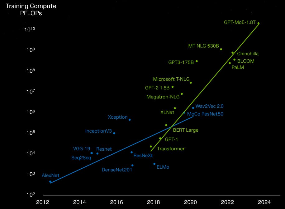
The opposing view for the future of the AI datacenter was provided by Broadcom. Rather than having everything vertically integrated, Broadcom is seeing a plug and play world, where components of different manufacturers can be swapped in and out of the AI datacenter at will from GPUs to CPUs, NICs and switches, communicating over open standard ethernet. The AI compute world Broadcom is seeing will be running on lower power custom silicon, also commonly known as ASICs, as opposed to Nvidia’s higher power general purpose datacenter GPUs. As training compute has been rising at a rate of 100x every two years (chart below, note the log scale), the argument for power efficiency is an important one:
So whereas Nvidia has more an Apple or Tesla-like approach, i.e. hardcore engineering combined with vertical integration to provide the best customer experience, Broadcom is seeing more an Android smartphone or Windows PC world for AI, i.e. software platforms running on hardware from any manufacturer. Now, both of these models have long and successful histories in tech as both have certain advantages. Vertical integration in the case of the Apple model and specialization for the Android model, i.e. every player in the value chain is focused on his task.
In this post, we’ll dive into both companies’ AI datacenter technologies and we’ll also do a financial analysis for both at the end. We’ll start with Broadcom as they provided a lot of detail on the lower level chip technologies powering the datacenter, before going into Nvidia’s more holistic and vertically integrated approach.
Broadcom’s open fabric AI datacenter
Broadcom’s COO started the AI event by moving away from the term GPU, which is the name popularized by Nvidia, while at the same time laying out the case for custom silicon:
“The AI accelerator, many people call it GPUs, some call it TPUs and others call it NPUs. For today, let's refer to it as XPUs. There are 2 ways you actually can develop these products. One, you can develop a general product that fits everybody's needs, which is great. However, if you're a consumer AI company and you're building these large-scale platforms, these general processors are actually too powerful in terms of power consumption and too expensive to deploy into their networks. Some of them have no choice today because they don't have the ability to do a custom capability. But the few that have the scale of billions of users, generating over $0.5 trillion in revenue, have that capability. And that's why we coin custom XPU or custom AI accelerator.”
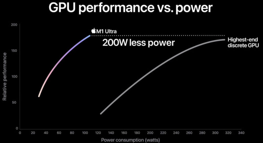
The company has three large customers now for their custom GPU business, it is well known that Google’s TPUs were the first, I’m guessing that Microsoft is the second one, and recently it has been speculated that either Meta or Bytedance would be the third. If my memory serves me well, Amazon would be working with Broadcom’s competitor Marvell. Designing these leading edge GPUs is an extremely R&D intensive business, with costs going into the billions of dollars. Nvidia mentioned they spent $10 billion on developing the overall Blackwell platform, more on this later. A lot of know-how and expertise are required, so this should be a good business with high barriers to entry. The main risk for both Broadcom and Marvell in this business would be that the internet and cloud giants start insourcing these activities more in the future, similar to how Apple has been designing ever more of their silicon in-house. Apple illustrates how custom silicon gives them performance benefits:
As also Broadcom is the strong player in both networking and other datacenter technologies such as connectivity — together with Marvell again — these AI datacenter revenue streams would start contributing 19% to Broadcom’s revenues this year:

This is Broadcom’s COO laying out the huge AI bull case for semiconductor investors, they’re talking with customers on how to build one million GPU AI clusters:
“If we go back to 2 years ago, a cluster that was state-of-the-art at the time had 4,096 XPUs, each XPU was a couple of hundred watts, and to interconnect 4,000 of these was fairly simple with a single-layer networking layer using our Tomahawk switches. In 2023, we actually built a cluster that is over 10,000 nodes of XPUs and it requires 2 layers of Tomahawk or Jericho switches. And this is the lowest power XPU in the industry today, less than 600 watts and using the latest technology. Now as you go towards 2024, we are going to extend this to over 30,000 and the objective of many of these consumer AI customers is how do we take this to 1 million.”
Here we get an overview of the key semiconductors involved in building these AI clusters:
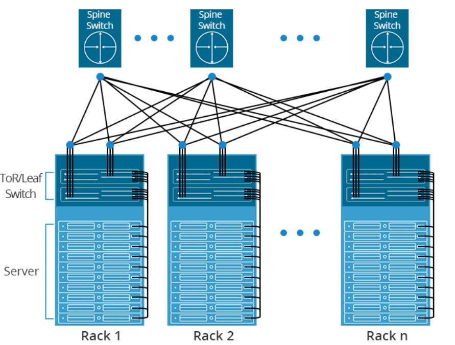
“So a cluster starts with an XPU. Typically, there's 8 of them in a server, unless you use Broadcom custom XPUs, you can have 12 or 24 of them. Because when you customize it, you can actually significantly cut the size and power. You have to connect these processors together and that function is called scaling up. That can be done through a PCIe switch, a proprietary switch, or even an ethernet switch. After that, you bring x86 or ARM processors as the control plane and that interconnect is done through PCIe switches. To get these to exit the server, you need network interface cards (NICs). So the basic building block is called the AI server or the AI node.
Now we have to take many of these servers and scale it out. That's the next step of architecting a cluster. You're going to have to use the best networking technology and we believe that the best networking technology is ethernet. As you scale up typically in 10,000 or 30,000 nodes, you need at least 2 layers of leaf and spine. And to do that, you need top of rack switches and spine switches, that's called the front end. Once you do that, you need to interconnect all of these with our optics products.
Remember the lowest power XPU today is ours, that's about 600 watts and the next one would be in the range of probably 1,000 watts. If you want to do 30,000 of these in a cluster, just the XPUs will use 30 megawatts of power. Most data centers, that's the maximum power they can give you. To solve this, we believe that this important inflection point in the industry has to be driven by open standards like ethernet, PCIe and other standard capabilities at the memory level. As you move beyond 10,000 and 30,000 XPUs, it becomes a distributed computing challenge and this will be solved with the best networking architecture that will be out there. Lastly, but most importantly, we need power efficient technologies.”
So the key point here is that due to the power constraints of a typical datacenter, Broadcom is arguing that AI accelerators will have to transition to custom silicon. These are optimized for particular AI workloads, thereby bringing in lower power and size requirements. The other important factor from an investment standpoint is obviously that a lot of networking and connectivity technology is involved, from switches to PCIe, which is again an area Broadcom excels at.
Let’s first go further into the custom silicon business, this is Broadcom’s head of ASICs detailing this unit:
“In 2014, we met a customer that decided to do something really cool in AI, and we developed an AI chip for them. As such, we started shifting resources and focus on AI. The benefit of custom silicon can be explained by a simple equation: performance divided by the total cost of ownership. The total cost of ownership is the cost of the chip, plus the cost of the power, plus the cost of the infrastructure to put it together. When you are one of these large internet companies, you have internal workloads that are very important for your revenue generation and for your applications. So if you customize the architecture of your accelerator, your bandwidth, the right ratio of I/O and the right ratio of memory, you can do those specific workloads much more efficiently than on general hardware. We work with our customers to customize the architecture that they have, to make sure that they can maximize performance for what they care about. And there's another really good effect, which is when you optimize hardware, you make it smaller and you make it cheaper. The other benefit, when you optimize power, you are optimizing power costs.
Let’s touch on the different aspects of an XPU. Number one, compute. We have developed a flow to optimize the architectural construction of that compute. We have several software engineers in my team, all they do is optimize the flow to build those accelerators i.e. really small, really fast and improving the TCO. Number two, memory. This is the ability to have HBMs and other memory solutions that have the right size, connectivity, cooling and testing and we're running these interfaces significantly faster than any standard or any competitor out there. Number three, I/O. We have created software tools that allow us to put together chiplets with wider and thinner I/O, to match the exact type of precision and ratio that the customer wants for their workloads. So we can do a 200 gig or a 100 gig PCIe and if they need another one next time, we just change it and we can go to production quickly. And we can give that to the customer before production so they can emulate the chip, they can simulate and they can solve all the problems. Number four, packaging. We can do 2.5D, 3D and silicon photonics, which is really hard. With 10 years of designing these AI chips, we have learned both our mistakes and our customers’ mistakes, and we have coded in software all these solutions to make sure that we're like a machine, with a lot of discipline and with a lot of automation to avoid errors.”
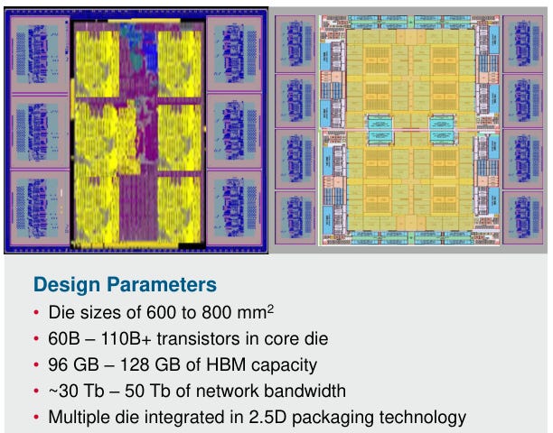
Below are two examples of AI accelerators designed by Broadcom for the internet giants. Obviously these are very advanced chips, large die sizes with up to 110 billion transistors in one die, 2.5D interconnected with 128 GB of HBM and 6 TB of networking bandwidth. Basically it’s a module that’s comparable to Nvidia’s current flagship H100 GPU.
You can see that Broadcom has over 150 tape-outs at the foundries’ leading process technologies, including 10 tape-outs at the latest 3nm:

At the company’s ‘22 ASIC event, they mentioned that this business has been growing at a 20% revenue CAGR. Obviously this is an interesting business, and the company can leverage all their knowhow and expertise from designing state-of-the-art semis over the past decades. However, the attraction of optimizing for one workload is also its major drawback. The reason that Nvidia has a market share of over 80% in AI workloads is that their GPUs not only perform spectacularly well, but they do so on the widest variety of workloads. As long as the field of AI keeps rapidly evolving, it makes much more sense to simply install a Nvidia cluster. Not only is it easier to deploy all your AI code on this cluster, but it makes you better future proof as AI workloads keep evolving over the coming years.
A recent example of the MLPerf test illustrates this, Nvidia’s H100 trumped Intel’s Gaudi on all workloads, and in some quite spectacularly so:

The other interesting AI datacenter exposure for Broadcom is their strong positioning in networking. This is the company’s head of switches on their networking strategy:
“This is a picture of Google's cloud about 20 years ago, what you see here is a bunch of commodity servers. They didn't pick the highest performing CPU, they picked the CPU that offered the best cycles per given cost and they connected it over ethernet. So they built the world's largest distributed computing system extended between data centers. What Meta showed is when they are running large AI workloads, anywhere between 18% to 57% of the time the traffic is just sitting in the network. That means that the GPUs are sitting idle.
Here's how we solve this problem. We have our Jericho 3 AI chip in production now, and you can deploy large clusters of up to 32,000 GPUs. These chips, they're 800 millimeters square — the largest that you can build in a reticle — and they have multiple HBMs. This is the architecture that Meta actually just recently published in a paper. They compared 2 clusters, one cluster based on InfiniBand — because there's a raging debate that somehow InfiniBand is magical, other than the fact that it's super expensive — and the other on ethernet. So they ran 2 clusters of 24,000 GPUs each and they tested it. Ethernet works fine, it's half the price and it doesn't melt down, it's 10% better performance than other alternatives. If you have a $2 billion to $10 billion infrastructure, 10% is about anywhere from $200 million to $1 billion and I'd be lucky if I got paid that much for the network. So for every dollar I spend, I save $1 and more.
The second way we solve this problem, we have the Tomahawk class of devices. Every 18 to 24 months, we are doubling the bandwidth. We are never in the habit of announcing products before we ship. I have seen others who announced products 2 years ahead of us, and we are shipping a year ahead of them. To get the bandwidth between the GPU and the switch, you need a NIC. This is Thor 2, our performance NIC which basically means we're focused on bandwidth. So GPUs need a lot of bandwidth and the NIC has to keep up.”
So Broadcom mentioned the two main types of their network switches, Tomahawk and Jericho. Tomahawk is a top-of-rack switch, it provides very high bandwidth to the servers at low cost. Jericho on the other hand can be used as a spine switch, it provides deep buffers to handle unpredictable workloads coupled with advanced telemetry, so you can get insights into the traffic.
Broadcom did some bashing of Infiniband as this is the networking technology promoted by Nvidia. The drawback is indeed that infiniband is higher cost, but the attractions are that it is extremely low latency and offers high bandwidth, and is thus very attractive for both high-performance computing as well as AI applications. Nvidia has also been moving into ethernet with its Spectrum X-branded ethernet tech to offer the best of both worlds, i.e. low cost and ubiquitous ethernet in parts of the datacenter where it makes sense, such as where traffic is flowing in and out of the datacenter i.e. North-South traffic. And high performing Infiniband where you connect all the GPUs together i.e. the East-West datacenter traffic.
Besides the scaling out of servers, the other part of networking are the connections inside the servers. Broadcom’s head of connectivity discussing developments inside the server:
“PCIe is the protocol to interconnect inside the server. Within a compute server, to the CPU you attach ethernet NICs, NVMe drives and storage adapters. What you'll find inside AI servers is multiple CPUs, 8 to 11 ethernet NICs, a dozen NVMe drives and 8 to 12 XPUs. So the point-to-point methodology does not work, you actually need to build a network inside an AI server. And the network of choice for that is PCIe as it's a very low latency. Having an open fabric allows you to pick and choose the components that you want.
There's 3 trays inside this AI server. The top tray has the CPU and the fabric, the middle tray has peripherals — that's where you'll stack up all your NICs, your NVMe drives — and the bottom tray, where a lot of the power and cooling is, is where you could put your XPUs. So PCIe is the internal fabric and ethernet as the scale-out fabric. So let's take the top tray, which has CPUs and the fabric, there's 4 heatsinks and each of these has one Broadcom PCIe Gen 5 switch inside. It's 4.6 terabits per second and you can attach up to 72 devices to it, either an ethernet NIC, or NVMe drive and so forth, and then that interconnects to the scale-out network utilizing ethernet. In some cases, the server is 15 inches tall and you may need to go further than the PCIe spec in terms of distance. A retimer basically extends the reach of the PCIe switch. Two weeks ago, we announced the industry's first 5-nanometer retimer chip. If you use our PCIe switch with our retimer, we can go 40% longer reach with 35% less power.
We introduced the first PCIe switch in 2003 when there was no AI server and we've been first to market for every generation of PCIe for the past 20 years. Now starting in Gen 4, that's when people started to build up AI servers and needed an internal fabric. Now we need to accelerate the cadence and go faster to the new protocol speeds. So we're shipping in volume PCIe Gen 5 switches today, which power the vast majority of the industry's AI servers, across both custom and merchant accelerators. We're going to be sampling PCIe Gen 6 switches at the end of this year. So we had 8 years between Gen 3 to Gen 4, 4 years between Gen 4 to Gen 5, and two years between Gen 5 and Gen 6. And now we're going to 1-year cadence.”
Broadcom illustrated the network of components inside the AI server, connected together via PCIe:

So this is clearly an interesting business, with AI, the number of connections inside the server has been exploding and we have an aggressive roadmap to increase the performance of these PCIe connections, meaning that few players will be able to compete here due to the R&D intensity.
Finally, Broadcom’s head of high-speed links provided an interesting discussion of where to use copper cables vs fiber optics in the construction of an AI cluster:
“If you go into this 1 million AI GPU cluster, you will find there are 10 million high-speed links. And these links are 400-gig, going to 800-gig and maybe 2 years down the road, it's going to be 1.6 terabits per second. So 400 gig is made up of 4 lanes of 100 gig, tomorrow, it will be 4 lanes of 200 gig and thereafter, it will be 8 lanes of 200 gig. So the bandwidth of these links actually doubles every 2 years and if you look at the sheer number of these links, these are the number two source of power and cost in an AI cluster, so it's very important.
If you take those 10 million links, a predominant portion of that today are copper. They are either on a backplane or they are on a direct attached copper cable within the rack. Their reach is about 5 meters or so and they have the lowest power and lowest cost. If you have to go beyond 5 meters, you have to use optics but they have the highest power and the highest cost. Our objectives are one, how do we make sure that as many links stay on copper as possible and then second, whatever links don't stay on copper, how do we reduce the cost and power for those links.
On the copper links, the technology that we use to drive these is SerDes and these cores are embedded inside a Tomahawk switch, the XPUs or the NICs that we have. Peregrine, which is our leading 5-nanometer and 100-gig SerDes, we did something very unique here. We built a native capability for optics so that you don't need to have a DSP or a retimer, you can actually drive optics directly from the SerDes itself and so that enables a very disruptive use case like CPO (copackaged optics). So this SerDes is available in every product that Broadcom will build, it may be switches, routers, XPUs, NICs,..
Today, we have actually some news that we want to share, our next-generation SerDes, codenamed Condor. It's built on 3 nanometer and it has very long reach, everything in the rack is pretty much covered without any retimers.”
The company also provided some more details on a variety of optics technologies they’re working on. Broadcom owns two fabs that manufacture optic components, one in Pennsylvania and one in Singapore. In the illustration below, the golden connections are where you use the optics. Basically, these are the longer distances where you have to travel further than 5 to 10 meters, for example, from a server to a switch:

And we got some examples of where the company has been introducing co-packaged optics:

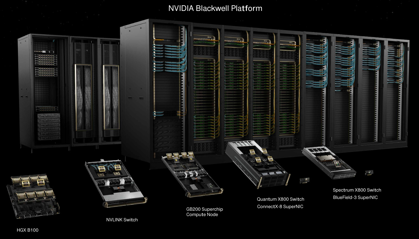
Nvidia’s integrated AI factory
The theme of the undisputed AI champion’s event was really ‘Nvidia everywhere’ i.e. a vertically integrated Nvidia factory powering all AI workloads. The company presented their new flagship GPU, the B100, which also has a version with an integrated CPU on the same board to handle certain workloads. Then there was the NVLink switch to handle low latency communication between GPUs within a server, the Infiniband X800 networking switch, the Infiniband SuperNIC, and we also got respective products to build a network based on ethernet. As discussed above, Nvidia uses NVLink and Infiniband to connect GPUs together, and Spectrum-X ethernet to manage data flows in and out of the datacenter. All of these products can be purchased separately or as the vertically integrated Blackwell platform:
So anyone who was betting that Nvidia would become a large market share donor in AI in the coming years, this isn’t going to happen anytime soon. While AMD will take some share, this will remain fairly limited at around 5% to perhaps 10% this year, and this is mostly just a function of Nvidia’s solutions remaining in short supply. And at the end of the year Blackwell will be released so if you can get your hands on this GPU, there shouldn’t be any reason to go for an AMD MI300 afterwards.
Needless to say, Nvidia’s new Blackwell platform is a computing beast, boasting 208 billion transistors per AI superchip and of which 576 can be interconnected together via NVlink, effectively forming one giant GPU with very low latency. But perhaps the most interesting feature is that these GPUs support 4 bit floating point calculations vs the previous 8 bit version. This means that each real number in AI calculations will only need 4 bits, effectively doubling the chip’s memory capacity as well as making it twice as fast. As I understand it, this feature will mostly be used in inferencing, as 4 bits is sufficiently precise here.

Another interesting innovation is the RAS engine, which is a built-in self testing system. This is Jensen detailing RAS:
“A supercomputer runs for weeks on end with many components working at the same time. The probability of them all working continuously is very low, zero. So we checkpoint and restart as often as we can, but if we have the ability to detect a weak chip or a weak node early, we can retire it and swap in another processor. That ability to keep the utilization of the supercomputer high is super important. And so we put in a RAS engine, a reliability engine, that 100% self-tests every single gate, every single bit of memory. It's almost as if we ship with every single chip its own advanced tester.”
Additionally the company is addressing the bandwidth problem in AI networking with better compression algorithms. This is Jensen on the topic:
“Decompression, moving data in and out of these nodes when the compute is so fast becomes really essential. And so we've put in a compression engine and it effectively moves data 20x faster in and out of these computers. These computers are so powerful that the last thing we want to do is have them be idle. And so all of these capabilities are intended to keep Blackwell fed and as busy as possible.”
The below chart illustrates how the computing power of Nvidia’s superchips has been evolving. Basically every two years, computing power goes up around 5-10 fold:

And when Nvidia bundles this computing power into a rack, this is what you get:
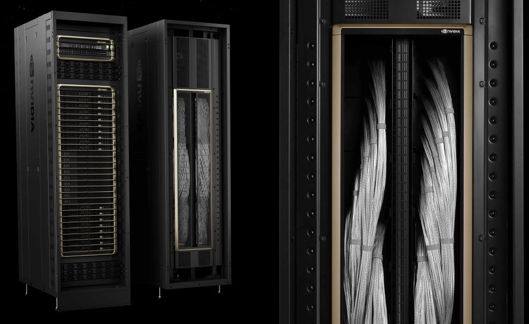
Jensen explains the new DGX Blackwell:
“I delivered the first DGX-1 to OpenAI and it was 170 teraflops, that's 0.17 petaflops. So this is now 720 petaflops, almost an exaflop for training and the world's first 1 exaflop machine in one rack. There are only a couple of 2, 3 exaflops machines on the planet and so this is an exaflops AI system in one single rack. Take a look at the back of it, the DGX NVLink spine, 130 terabytes per second goes through the back of that chassis. That is more than the aggregate bandwidth of the Internet so we could basically send everything to everybody within a second. That’s 5,000 NVLink cables, in total two miles. If we had to use optics, we would have had to use transceivers and retimers and those transceivers and retimers alone would have cost 20,000 watts. As a result, we did it completely for free over NVLink Switch. This entire rack is 120 kilowatts, so that 20 kilowatts makes a huge difference. It's liquid cooled, what goes in is 25 degrees C, about room temperature and what comes out is 45 degrees C, about your jacuzzi. When somebody says GPU, I see this. Our GPUs now are 600,000 parts and 3,000 pounds.”
Jensen then detailed the training times and power requirements for their platforms:
“If you were to train a 1.8 trillion parameter model, it took about 3 to 5 months or so with 25,000 Ampere GPUs. If we were to do this with Hopper, it would probably take something like 8,000 GPUs and it will consume 15 megawatts in 90 days. If you were to use Blackwell to do this, it would only take 2,000 GPUs during the same 90 days, but only 4 megawatts of power. And that's our goal, to continuously drive down the cost and the energy.”
On the software side, one of the most interesting announcements was that Chinese automotive giant BYD will be implementing Nvidia’s self-driving system powered by Thor, Nvidia’s self-driving chip. In the future, self-driving software is likely to become a market going into the hundreds of billions of dollars, so the companies who can successfully capture this market will see their valuations increased with over a trillion dollar. This is a space definitely worth monitoring.
An even more exciting space would be a robotaxi market, where robotaxis taking a 15% share of the global miles driven would result in nearly a trillion dollar in revenues for the autonomous vehicle (AV) system provider e.g. Nvidia or Mobileye, assuming a 20% take rate of the robotaxi company’s revenues e.g. Uber:

Nvidia is using the same Omniverse digital world — which they use to train self-driving cars — in the training of humanoid robots. Jensen on the company’s capabilities in robotics:
“We're creating the entire stack, a foundation model that learns from watching video, human examples, and we then created a virtual gym for it, called Isaac reinforcement learning gym. This allows the humanoid robot to learn how to adapt to the physical world. And then an incredible computer, Thor, the same computer that's going to go into a robotic car, will run inside humanoid robots and it’s for transformer engines.”
So Nvidia isn’t purely focused on AI datacenter acceleration and inferencing, but long term they’re are looking to play in potentially big markets such as autonomous driving systems, robotaxis and robotics.
Financials — NVDA share price of $900 at time of writing and $1,308 for AVGO, both trading on the Nasdaq
Nvidia’s quarterly revenues and quarter-on-quarter growth rate are presented below, together with the sell side’s estimates for the coming quarters.

Looking at ‘26 and ‘27 below, Wall Street’s estimates don’t look aggressive, given that other sources see the AI server market growing at more than a 30% CAGR. Currently the shares are trading at a reasonable 32x next year’s EPS, combined with what is a modest SBC payout, at around 0.15% of the current market cap.
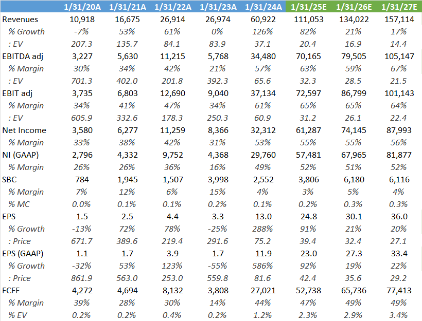
Also compared to Nvidia’s trading history, valuation on a PE basis still looks reasonable currently. The valuation is basically roughly in line with the shares’ trading history over the last 7 years:

The main risk with these shares is that due to the unprecedented boom in AI capex, at some stage we’ll hit a cyclical pullback resulting in Nvidia seeing substantial revenue declines for a number of quarters. However, given that Broadcom and its customers are talking about one million GPU clusters versus the current number of around 30,000 GPU clusters, the long term demand picture looks extremely strong. So I’m still on the side that the risk-reward is attractive enough here to hold the shares.
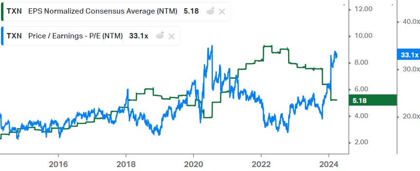
Note that as investors grow more comfortable with the long term story, this will help the trading multiple expand should a shorter term cyclical pullback occur, helping to alleviate the impact on the share price. So basically this means that as shorter term EPS go down, the market will reward the shares with a higher PE as investors are willing to look through the cycle. A good recent example of a situation like this is Texas Instruments:
Broadcom is exposed to a long term attractive story in datacenter semiconductors as discussed above. However, it has become a very diversified beast with also infrastructure software becoming an important part of the mix due to the VMware, CA Technologies and Symantec acquisitions. So Broadcom has become a serial acquirer in tech really. That said, valuation is not overly expensive at 28x ‘24 PE combined with a 3%-plus FCF yield, for a company which should be able to generate double digit top line and EPS growth:

Although compared to its recent trading history, a 26x next-twelve-months’ PE is at the top end of the range. A re-rating has been justified however given its attractive AI and datacenter semiconductor exposures. In my opinion, these shares will likely continue to be a solid long term investment.

For investors looking for income, Broadcom also has a 1.6% dividend yield and the company is committed to keep returning a growing amount of cash to shareholders:

If you enjoy research like this, hit the like & restack buttons, and subscribe if you haven’t done so yet. Also, please share a link to this post on social media or with others who might be interested, it will help the newsletter to grow, which is a good incentive to publish more.
I’m also regularly discussing tech and investments on my Twitter.
Disclaimer - This article is not a recommendation to buy or sell the mentioned securities, it is purely for informational purposes. While I’ve aimed to use accurate and reliable information in writing this, it can not be guaranteed that all information used is of this nature. Before making any investment, it is recommended to do your own due diligence.
Tech Fund, excellent coverage. 🔥👍🏽
Great read, thank you.
I’m fascinated to see how this level of investment in innovation (Nvidia) actually unfolds.