

Navitas, outlook post investor day
Navitas, outlook post investor day
An overview of the GaN space

Power semiconductors, SiC vs GaN
Power semiconductors are everywhere, as they are used in all applications where electricity needs to be controlled or converted (from AC to DC for example). Therefore, they will be essential as we transition the economy from being powered by fossil fuels to one running on green energy, for example solar and wind power in combination with large scale battery storage.
Traditionally, power semiconductors were silicon based. However, there are two materials showing much greater efficiency at handling power, i.e. silicon-carbide (SiC) and gallium-nitride (GaN). The advantages of these are numerous, but essentially, due to much lower heat generation and lost power, battery lifes of equipment such as electric vehicles and smartphones can be increased. As well as that devices can be made smaller, e.g. thinner TV screens.
SiC is being used to handle high voltages, such as in electric vehicles, trains, wind and solar, and industrial robots. GaN on the other hand is being inserted in low voltage appliances such as laptops, TVs, smartphones and other home appliances. Although the material is now also seeing adoption at mid-level voltages where it will have to compete with SiC, or can be used in combination with SiC, such as in the data center, residential solar, and EVs. Navitas provides the following overview chart:
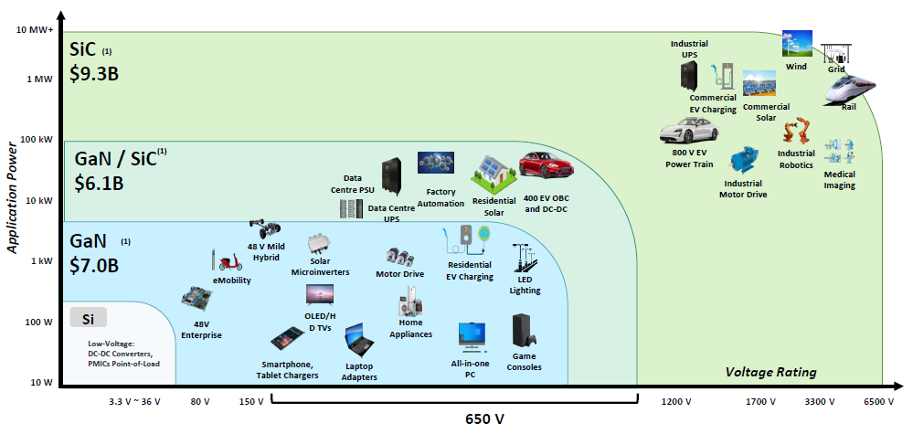
SiC is generally expected to be the far larger market, and also as the life cycles of these types of products is much longer, as a car model can be in production for 10 years vs 2 years for a smartphone, SiC should be the more interesting market of the two. This is a key reason why I reviewed Wolfspeed previously, a pioneer in SiC across the entire value chain, from wafer manufacturing to semiconductor fabrication. As well as that both SiC and GaN should remain high-growth markets for quite a while:
Generally, semiconductor companies providing to shorter lifecycle-type products such as smartphones are typically seen as lower quality. A smartphone model is only in production for a few years and in the subsequent generation, you might lose the slot for your semi. Suppliers to Apple especially will lead a nerve-racking life, as Apple has increasingly been taking semiconductor design in-house. However, even in this very competitive space, we have seen some highly successful semiconductor business models, with companies such as Qualcomm and Arm being prime examples. Even a less differentiated supplier like Dialog was taken over by Renesas and investors did great in these shares.
Navitas’ recent investor day
Navitas’ CEO started by explaining the benefits on GaN:
“Gallium-nitride and silicon-carbide are widely known as the key technologies to displace silicon and make the transition happen. The frequency is the key to GaN and SiC switching fast, because more than half of the bill of materials (BoM) of almost all power systems are in the magnetic and mechanical components — the EMI filters, the transformers, the inductors, the PCBs on the mechanical side, the housing plastic or metal — all of that is usually half or more of the system. The faster we switch the power device, the more we shrink the size, weight, and cost of that other half of the BoM. So it’s actually far more important to get the frequency up and reduce the cost of the rest than it is to take the cost of the GaN or SiC chip down. It allows you to have less energy burned up as heat. So you spend less money, time and effort on thermal management.”
As GaN can switch much faster than purely silicon-based power semiconductors, one of it first applications has been in fast charging. The company gave the example of how one of their clients built a smaller fast charger with Navitas’ new GaN module:

Navitas’ CEO detailing this market:
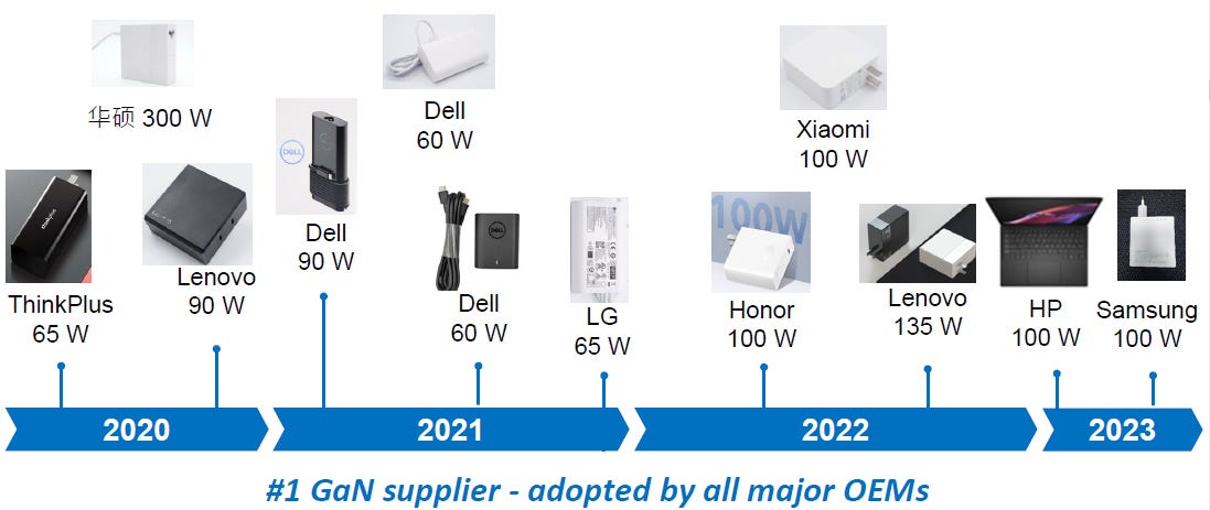
“Over 250 GaN chargers are shipping in production, all 10 of the top 10 smartphone and laptop guys are already in production with Navitas GaN Fast chargers. By leveraging our proprietary technologies, we have created a 150-watt multi-port charger that is 38% smaller than Apple’s 140-watt single port charger, but it’s powerful enough to charge 2 laptops at high speed or power up to 4 devices simultaneously.”
Obviously Navitas has an extremely strong position in this market and attractively, there is plenty of room for growth as overall adoption of GaN-based chargers is still only at 10%.
While the mobile charging market was the initial application of GaN, Navitas highlighted their $1.25 billion pipeline of programs expected to go into production in the next several years. This will shift the revenue mix towards more interesting markets such as solar, EVs, industrials, data centers, and home appliances. The estimated pipeline was raised with $500 million over the last 7 months alone, highlighting the strong momentum the company is seeing:

These new markets have been taking some time to come online as new chips have to undergo rigorous testing before they can get a win into a new product line. This is especially the case for EVs as a vehicle can be on the road for 10-15 years and under a wide variety of conditions, from the Canadian winters to the hot desert of Dubai.
The company’s CTO discussed the pipeline at the capital markets day:
“We’re taking conservative lifetime estimates for these different market segments, meaning 1 to 2 years in the mobile and consumer space, and 3 to 5 years in the other market segments. In EVs, we’re targeting diverse applications, starting with on-board chargers as well as roadside chargers. Today, we have significant SiC revenue in tier 1 EV players and we expect to ramp our GaN revenue in 2025. Today, we have our SiC technology in more than 50% of roadside chargers in the United States through our partnership with SK Signet. We are expanding and growing that footprint into other partners in roadside charging, and we’re working closely to develop solutions that will take the current 350 kilowatt state-of-the-art roadside charger from Tesla up to 1 megawatt or more.
Solar and energy storage, we have multigenerational GaN designs currently underway with the microinverter market leader, and we have GaN programs kicked off in the North America string inverter market leader.
We’re engaged with 7 of the top 10 home appliance manufacturers and we’ll start to see revenue late ‘24, ramping in ‘25 and beyond. We have strong and broad customer engagements across industrial applications: pumps, air conditioning, heat pumps, industrial motor drives. Specifically, we have a heat pump design in a top 3 player in that market, that could be $25 million to $50 million in just that design alone. And then we have 2 out of the top 3 industrial pump players that are currently designing with our solutions.
So data center is a very exciting space. We see AI driving and pulling the power density and efficiency ever higher, and that’s a perfect fit for Navitas. We have reference designs that we can leverage and we have engagements with the top 3 power system players. And we’re going to continue to drive that bleeding edge tier of power density and efficiency with the major data center providers in the US, as well as in China and around the world.
We’re now shipping in 10 of the top 10 mobile players, including the 5 major mobile phone players as well as the 5 largest notebook OEMs. In China, Xiaomi and Oppo expect that at least 30% of their mobile phone chargers will be GaN-based in 2024. These are not niche phones or expensive phones, these are mainstream phones with great battery life and huge screens. So it’s pretty compelling, having a battery charger taking less than 10 minutes to go from 0 to 100.
We’ve had some good successes in desktop PCs, gaming PCs, but now we’re seeing real traction in the gaming console market. We’re actively engaged with the top two console players worldwide for future generation development. They can leverage the smaller sizes to make more compelling products.
TVs are getting larger, but they are also getting thinner while requiring more power. That’s a perfect fit for our integrated GaN IC. So we have multiple tier 1 OEM design engagements underway, where we expect that we’ll be announcing shipping starting in the first part of ‘24.”
The company also mentioned a competitive advantage in chip size, Navitas’ CEO going into this:
“Also chip size is important. It’s not just about wafer price, our chips are 20% to 50% smaller across SiC and GaN compared to the majority of our competitors.
We spent a lot of time hiring the best engineers for each application, digging into the system requirements, understanding how to optimize for that, and now creating joint labs with our customers where we can co-develop each of these applications and drive that final phase of customer adoption.”
The final point of building labs around the world is an interesting one, as they will enable forming deep relationships with their customers.
They also showed a lot of the logos they’re working with, which included interesting names. For example in EVs, there is BYD, BorgWarner and Hyundai:

In solar, we can see both Enphase and SolarEdge, as well as CATL:
In data centers, there are Dell, HP, AWS, Azure etc:

In mobile, we have Apple, Samsung, Xiaomi and Sony.
On the last earnings call, the company discussed a win with Samsung:
“Navitas GaN has been adopted at Samsung to power the latest Galaxy S23 among other models, and is already contributing to our Q3 and Q4 revenue ramp.”
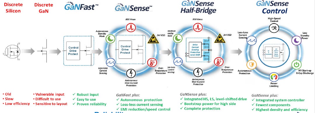
The company also highlighted well how their GaN solutions are evolving from generation to generation, from basic discrete semiconductors (i.e. one switch) to complete modules. For example, they highlighted a module which includes a controller to switch the device off if the current becomes too high. This was all packaged in a tiny 6 by 8 mm module. Innovations like these have been realized both from internal R&D as well as via acquisition.
A good example of how they’re innovating was given on the last earnings call:
“Potentially the most exciting and impactful announcement is a breakthrough innovation called bidirectional GaN. Now for the first time, GaN ICs can operate quickly and efficiently, conducting and blocking currents in both directions. This bidirectional GaN allows the replacement of up to four discrete power transistors, providing similar functionality while dramatically reducing component count, cost, and complexity, and delivering the speed and efficiency benefits of gallium nitride. We believe this invention has the potential to create innovative advances in energy storage, grid infrastructure, motor drives, and many other emerging topologies across multiple markets.”
Yole’s industry analysis
Research house Yole does great work on semiconductors and they provided a nice overview of the GaN supply chain, from substrates, epitaxy, manufacturing, design, and packaging to the end-clients which utilize the semis into their systems:
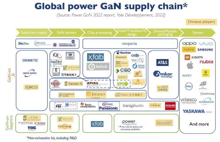
We can see that in design, Navitas will have to compete with numerous competitors, including Chinese players and more vertically integrated players such as Infineon, STM and Texas Instruments. From Semiconductor Today:
“Focusing on the Chinese ecosystem, the government has supported more investments from GaN players. Notably, privately owned Innoscience is investing more than $400 million to expand its 8-inch wafer capacity from 10,000 to 70,000 wafers per month by 2025. A domestic supply chain for GaN power is well developed, especially for the consumer market.”
I’m less concerned about Chinese competition as we seem to be moving towards a bipolar tech world, one where Western companies prefer to avoid Chinese components in their supply chains and vice versa, with Chinese manufacturers preferring domestically sourced technologies. But even taking the Chinese players out, we can see that Navitas still will have to face easily around 10 or more competitors.. And as we saw this week, also Japanese semi powerhouse Renesas is aiming to enter the market with its acquisition of Transphorm. However, I think it is possible that US authorities will block this deal, as they did with Infineon’s attempt in taking over Wolfspeed a number of years ago.
Looking at 2021 GaN market shares, Yole has Navitas as the number two player, positioned after Nasdaq-listed Power Integrations:

Earlier we saw that Navitas estimated the GaN market to grow to above $7 billion by 2026, however, Yole provides much more conservative assumptions, estimating the market to grow to $2 billion by 2027:

Yole continues to see strong GaN growth beyond 2027 coming from EVs and the industrial market:

So this might explain the difference between Navitas’ and Yole’s market sizing estimates. As we saw above, Navitas is already working with EV and industrial players on designing GaN solutions, so it looks like the company is bullish on this market coming online sooner. However, below in the valuation, we will take more conservative assumptions.
Starting a Silicon Carbide (SiC) business
As already mentioned above, the company has also entered SiC which is today becoming an increasingly crowded field. I’ve probably seen around 15 US, European or Japanese semiconductor manufacturers announcing over the last few years to invest in SiC fabs. On top of that, also local Chinese players are looking to break in. So we could potentially be looking at 20 to 25 players in this field.
Overall, I’m not really enthused about Navitas entering here, although it will be to their advantage that they’re making use of outsourced, analog-type foundries for manufacturing. This means that they won’t have to make large investments themselves, reducing the risk for shareholders.
Navitas will be making a limited investment of $20 million to run their own epitaxy reactors, which is where a thin layer of SiC crystals are deposited on a SiC substrate, after which the wafers can be used in manufacturing. With epitaxy, you can precisely control the properties of the chip, with conductivity being one example.
The company acquired their SiC technology, and their new head of SiC actually gave an interesting presentation:
“I came to Navitas in 2022 through the GeneSiC acquisition, where I spent 15 years working on SiC power devices. All of our 20 key people have made the transition to Navitas. GeneSiC has the widest SiC MOSFET portfolio in the world, we have parts ranging from 650 volts all the way to 6,500 volts, a total of 60-plus MOSFET products. Ranging from discrete parts, to bare dies and power modules.
The first SiC MOSFETs that were introduced by Wolfspeed in 2011 were planar, similar to what was done in silicon and easier to manufacture. In silicon, the limitations of planar were overcome by moving to trench gate architectures. Unsurprisingly, the same has been attempted in SiC and there are many vendors who have already offered SiC trench MOSFETs into the marketplace. What is common to all of these is that they need extremely complex manufacturing lines, often requiring very exotic process steps. Typically, trench has 30% to 50% more process steps than planar. Consequently, they are prone to suffering from lower yields.
What we have done at GeneSiC is really bring the best of both worlds together. We’ve taken the best features of planar, the best features of trench, and combined those into what we call a trench-assisted planar-gate MOSFET. This MOSFET is manufacturing-wise similar to planar, but performance-wise, it can rival or even exceed trench. What you get is lower losses and a cooler operation.
So here is our product roadmap for the next 2 years. In the early part of 2024, we plan to introduce our Gen-3 Fast SiC MOSFETs, Gen-5 MPS diodes, followed by Gen-4 SiC MOSFET chips, which are specifically designed and targeted for EV traction applications. We follow that with topside cool SiC MOSFETs. Our very first SiC module offering will be the SiC-PAK. Later on, in 2025, we plan to unveil and release our proprietary SDC power module, specifically targeted for EV traction applications, top cool power modules will follow for OBC (on-board charger) applications. And finally, we plan to release ultra-high voltage SiC modules at 3.3 and 6.5 kilovolts.”
As a potential negative, Navitas is currently on 6-inch substrates whereas some competitors are moving to 8-inch. The size of the wafer is important as the more dies you can manufacture on a single wafer, the lower the cost per chip. So the company could have a competitive disadvantage here over the long run. However, 8-inch SiC wafers are still novel so Navitas’ view is that it currently remains advantageous to stay on 6-inch:
“So we are in 6-inch wafers, 8-inch wafers are very expensive still. The cost per square centimeter of 8-inch is much higher, so 6-inch is actually the more cost-effective process at the moment. And our yields are quite high, thanks to this trench assisted planar process, it is a simple process. The first thing we do is ask our customers, please test our devices because you’re going to see the advantage, and that’s going to give us the opportunity to get some benefit ourselves in terms of our pricing.”
So with the final point he means that with increased scale, they will be able to bring pricing down. Also, as 8-inch technology becomes more mature, there is scope for Navitas’ foundry partners to move over to this technology, more on this in a bit. So at this stage, I wouldn’t be overly concerned that they’re still on 6-inch.
At the investor day, Navitas also had a series of clients presenting and one that stood out was DGMatrix, a manufacturer of EV and microgrid solutions:
“We tested a number of devices, some of them from very large companies, and we found Navitas performance for the on-time resistance of the SiC device to be best-in-class for whatever we’ve tested today. That gives us an industry-leading efficiency of 95% to 97%. In addition, the high-voltage breakdown is astounding, how much it can take in spikes, which really points to the resiliency when you put this on dirty grids. When you’re going to put this on a dirty grid in a developing country, you’re going to see a lot of sags, surges and spikes.”
The semi and SiC cycle
SiC is especially exposed to the automotive end-market and a number of semi companies have been downguiding numbers to this area, highlighting a cyclical pullback in this market, also as semi inventories in the channel are still high. Testing equipment manufacturer Aehr gave an update how this relates to the SiC market in particular:
“In just the last 60 days, we’ve seen how the slowing of the growth rate of the electric vehicle market has had a negative impact on the timing of several customer orders and capacity increases. For clarity, we do not see the silicon carbide market actually decreasing, only a slowing of the growth rate.”
Given that this business is still nascent for Navitas, I’m not expecting much impact from this. But should we see broader cyclical weakness in semis overall, naturally this will provide a headwind for the company in the coming quarters. Meaning that due to the company’s current high-growth trajectory, we’d be looking in that scenario at a slowing of the overall growth rate.
Manufacturing
As already discussed, the company is using outside foundries for both the SiC and GaN semiconductor manufacturing. In Navitas’ case these are TSMC for GaN and X-FAB for SiC. The company’s CEO discussing their manufacturing strategy:
“We have the best design and a really low-tech manufacturing requirement, you can build this in old, 6-inch factories, 0.35 micron, that’s a beautiful thing. These fabs were built 20, 30 years ago, are fully depreciated, low-cost, with often excess capacity as silicon has moved onto 8-inch, 12-inch, and more advanced nodes. TSMC is building our GaN in their oldest factory in production today, Fab 2. X-Fab is working from Texas with a fab that was built back in the 80s. So now we have more options, with silicon fab guys that love to upgrade their fabs to GaN and breathe new life into them for the next 10 or 20 years.
So we mentioned early in ‘23, we signed an agreement with X-Fab for a 500% increase in capacity and that’s throughout ‘23 and ‘24. In a similar way, TSMC expanded the GaN capacity and tripled it, this finished in ‘22.
We’re shipping all we can build on GaN, the orders keep coming in with very short lead times.”
According to Semiconductor Engineering, X-Fab has already moved to 8-inch :
“Today, some players already have 8-inch GaN-on-Si fabs — i.e. Innoscience and X-Fab — or they are moving to 200mm — i.e. Infineon, STMicroelectronics, Nexperia, BelGaN, and TSMC — in the coming years.
On the foundry side, X-Fab got a very early start. ‘As the first pure-play foundry, we offer customers the capability to process their highly efficient, high-voltage power devices on 200-mm-GaN-on-silicon wafers using our European CMOS production facility in Dresden, Germany,’ said X-Fab’s product marketing manager for SiC and GaN. ‘There is no specific or dedicated tool for the GaN wafers. All equipment is set up to handle both wafer materials, silicon and GaN-on-Si.’ ”
So Navitas could switch to X-Fab’s 8-inch fab as well over time, while the other foundry partner, TSMC, is in the process of moving over to 8-inch as well.
China controls the supply of gallium, a potential risk?
From the Nikkei:
“Gallium prices are surging after China said it would start requiring permits to export the key metal and other chipmaking materials in August, signaling a potentially significant impact on the industry.
The benchmark price for gallium in the U.S. and European markets reached $332.50 per kilogram on July 20, according to U.K.-based Argus Media -- up 18% from the end of June, before China made its announcement on July 3.
China produces 540 tonnes of gallium a year, or 98% of the global supply, according to the U.S. Geological Survey. The material is used in blue light-emitting diodes, the development of which won the Nobel Prize.
Gallium is also seen as the next big thing in power semiconductor devices for electric vehicles and smart grids, since it loses less energy than the more commonly used silicon.”
Gallium is sourced from bauxite mining, the primary ore of aluminum which often contains trace amounts of gallium. This bauxite is then shipped from Australia and other mining countries to China where it is processed into aluminum, during which the gallium can be extracted.
Digitimes Asia notes that China’s potential chokehold is not an issue as the gallium in GaN epitaxy is sourced from trimethylgallium, which is produced by Japan, Europe and the US. However, trimethylgallium is basically one gallium atom bounded with three methyl molecules (one methyl molecule is CH3), a very prevalent organic compound on earth — your body is full of it. My understanding is that the gallium to produce trimethylgallium is sourced from China..
So while China has not taken any actions so far — they’re only requiring export permits at the moment — which have been granted, the CCP could effectively cut the world off from gallium. My understanding is that this would result in the Western-aligned democracies around the world not being able to produce GaN wafers.. As the Biden administration has been ramping up export restrictions of advanced semiconductors and equipment, it seems likely to me that the Chinese will start retaliating at some stage. Especially as the green agenda is a core pillar of Bidenomics, blocking gallium supplies would be a mechanism to make the transition to a green economy more difficult, something which the Democrats desire.
On the flipside, we have a Chinese economy which has been sluggish as well, and with concerns of a possible credit crisis due to the high leverage in the system. These factors have been redirecting the Xi administration again towards a more business-friendly tone, with Xi’s recent visit to San Francisco to meet the American business elites as an obvious example. This could be a factor in allowing the exports of gallium to continue (for the moment?).
Financials, share price of $6.9 at time of writing, ticker NVTS on the Nasdaq
Obviously this remains a speculative investment to some extent as the business is still nascent and still burning cash. However, the burn is quite mild with only $32 million of FCF estimated to be lost during ‘23, while the business still has around $170 million in cash. The currently estimated pipeline of $1.25 billion should start translating into $200 to $400 million of revenues over the next few years, allowing the business to turn profitable.

Stock based compensation was around $50 million over the last twelve months, so we’re currently looking at around 4% of dilution per annum when comparing this number to the market cap.
In the below IRR calculation, I’ve tried to make reasonable assumptions to see what we end up with for Navitas. Taking a GaN market size far below Navitas’ estimate of $7+ billion but somewhat above Yole’s estimate of $2 billion, clearly investors can make a good return under such a scenario assuming Navitas can hold onto a 15% market share and will trade on a 6.5x forward EV-to-Sales multiple in ‘26.
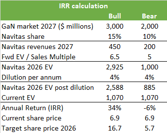
I’ve also factored in annual dilution of 4%. However, when the business turns free cash flow positive at some stage, they can use that cash to start offsetting dilution.
For comparison, I’ve also modelled in a bear case scenario which equally likely could play out. I’ve still factored in a decent multiple of 5x as the GaN market should remain high growth for quite some time, so I’m not seeing this stock move to a low multiple in the medium term. Also note that Renesas is taking out Transphorm at close to 10x forward revenues.
Looking at both scenarios, the risk-reward still looks to be on the upside. So I’m not uninterested in this name — they have a fairly strong position in GaN, although as a negative there are a large variety of players looking to compete, including the big semi names in this space. Additionally we have as a risk China’s control of the gallium supply.
Historically, in any high growth market which doesn’t have sufficient barriers to entry, as could well be the case in GaN and SiC, investors frequently have been burned as the industry struggles to generate sufficient margins. After such phases, these types of industries tend to consolidate, after which returns for investors usually turn healthy. Overall, I’m currently tracking the GaN and SiC markets as they remain interesting stories in semis, but I’m holding no positions at the moment.
My concerns on the competitive environment are reflected in Navitas’ gross margins, a 42% margin is not stellar for a semiconductor company, especially when you claim to have a differentiated product. Most good semiconductor companies will make gross margins north of 50%, and the really good ones above 60%.

Navitas reckons that in the long run, the business can move to gross margins of above 50% driven by a more advanced product portfolio, which would translate into operating margins of above 20%:

The company’s CEO discussing this:
“Silicon discretes have averaged sort of 30 to 50 points (of gross margins) depending upon where you are in the cycle. On the contrast, more integrated and differentiated analog ICs have commanded 50 to 70 points of margin. Long term, we still see our business as a blend of those two, which is why I think we’re trying to be realistic and say we’re somewhere in the 50s (long term).”
This may be possible, but naturally wait and see for the moment. If you believe that they can capture a large share in the GaN market while generating 50%+ gross margins, the shares should be a good investment.
Looking at peers, the more diversified ICAPS players typically trade on 2.5 to 4.5x forward sales, although the highest quality ones such as Analog Devices and Texas Instruments can trade on around 9 to 10:

If you enjoy research like this, hit the like button and subscribe. Also, please share a link to this post on social media or with colleagues with a positive comment, it will help the publication to grow. All shares are appreciated.
I’m also regularly discussing tech and investments on my Twitter.
Disclaimer - This article is not a recommendation to buy or sell the mentioned securities, it is purely for informational purposes. While I’ve aimed to use accurate and reliable information in writing this, it can not be guaranteed that all information used is of this nature. The views expressed in this article may change over time without giving notice. The future performance of the mentioned securities remains uncertain, with both upside as well as downside scenarios possible.